Pad Cell: Difference between revisions
No edit summary |
|||
| (25 intermediate revisions by the same user not shown) | |||
| Line 1: | Line 1: | ||
A typical pad cell consists of driver logic, ESD protection and a bonding pad, which essentially just is a "large" metal square, big enough to fit a bonding ball needed to attach the bonding wire or solder it to a PCB (flip chip bonding) or onto another carrier substrate chip (chiplet assembly) | A typical pad cell consists of driver logic, ESD protection and a bonding pad, which essentially just is a "large" metal square, big enough to fit a bonding ball needed to attach the bonding wire or solder it to a PCB (flip chip bonding) or onto another carrier substrate chip (chiplet assembly) | ||
[[File:Padcell.png|none|thumb|302x302px|Pad Cell in Magic editor]] | [[File:Padcell.png|none|thumb|302x302px|Pad Cell in Magic editor]] | ||
The schematic of the pad cell can generally be broken down into purely combinatory and active analog design components.[[File:Pad Cell Schematics.png|none|thumb|Pad Cell Schematics]]Where we have the two standard logic cells, and inverter and a NAND2 gate (red), transmission gate with level shifting (yellow), a tri-state driver, with 1, 0 and Z (high impedance).(green) and the transistors for pull up and pull down. | |||
== Driver Logic == | == Driver Logic == | ||
| Line 16: | Line 19: | ||
* Setting whether the driver should be active at all (Output Enable) | * Setting whether the driver should be active at all (Output Enable) | ||
* Provide a state engine or other means for configuring the termination resistance to ground. | * Provide a state engine or other means for configuring the termination resistance to ground. | ||
=== INV (Inverter) === | |||
[[File:Inverter.png|none|thumb|An Inverter gate]] | |||
{| class="wikitable" style="text-align:center" | |||
|- | |||
! colspan="2" | Inverter truth table | |||
|- bgcolor="#ddeeff" | |||
|colspan=1|'''Input''' || '''Output''' | |||
|- bgcolor="#ddeeff" | |||
| A || NOT A | |||
|- | |||
! style="color:red"| 0 | |||
! style="color:green" | 1 | |||
|- | |||
! style="color:green" | 1 | |||
! style="color:red"| 0 | |||
|} | |||
=== NAND2 (NAND gate) === | |||
[[File:NAND2 Gate.png|none|thumb|A NAND2 gate]] | |||
{| class="wikitable" style="text-align:center" | |||
|- | |||
! colspan="3" |NAND gate truth table | |||
|- bgcolor="#ddeeff" | |||
| colspan="2" |'''Input''' ||'''Output''' | |||
|- bgcolor="#ddeeff" | |||
|A||B||A NAND B | |||
|- | |||
! style="color:red" | 0 | |||
! style="color:red"| 0 | |||
! style="color:green" | 1 | |||
|- | |||
! style="color:red" | 0 | |||
! style="color:green" | 1 | |||
! style="color:green" | 1 | |||
|- | |||
! style="color:green" | 1 | |||
! style="color:red" | 0 | |||
! style="color:green" | 1 | |||
|- | |||
! style="color:green" | 1 | |||
! style="color:green" | 1 | |||
! style="color:red" | 0 | |||
|} | |||
== Input Buffer/Level Shifter == | |||
The transmission gate has the purpose of making sure that the input signal is being shifted to the logic levels of the internal logic, for instance 3V3 external logic levels to 1V8 internal logic. | |||
[[File:Transmission gate.png|none|thumb|Transmission Gate Schematics]] | |||
In addition, it contains additional polarity, over voltage and current protection. | |||
== Driver circuit == | == Driver circuit == | ||
| Line 21: | Line 76: | ||
In order to make a chip do something useful driver circuits need to be implemented which can provide the power needed for actually driving loads like making an LED blink or driving a small DC motor. | In order to make a chip do something useful driver circuits need to be implemented which can provide the power needed for actually driving loads like making an LED blink or driving a small DC motor. | ||
[[File:Output Driver.png|none|thumb|Driver Circuit Schematic]] | |||
This is being done in the driver circuit through [[Fingered Transistors]] which turn the low power logic states at its inputs into a state which is useful to the outside world. | |||
In the schematic above, the output transistors M7 and M8 are responsible for ultimately driving the loads attached to a pad and as such will be much larger than their driving transistors (M1=M6). M7/M8 are [[Fingered Transistors]] | |||
== ESD protection == | == ESD protection == | ||
The figure below shows an example of the rail-based protection in which the primary dual diodes (D1 and D2), the secondary dual diodes (D3 and D4), the NMOSFET power supply clamp are employed. | |||
[[File:ESD layout.png|none|thumb|200x200px|Example ESD layout done in Magic]] | |||
The power clamp provides a current path from the power supply pad to the ground pad during various ESD events. | |||
It's the simplest form of the RC-triggered power supply clamp, where the RC network and the inverter chain are designed such that the NMOSFET (M1) remains off during normal operation and turns on during an ESD event. This NMOSFET should be wide enough to handle the ESD current when it is on during an ESD event. | |||
[[File:Rail-based ESD Protection.png|none|thumb|Concept of rail-based ESD Protection. ESD current is redirected to the VDD power rail and then shunted to GND by a power clamp.]] | |||
An example layout found in one of the opened up PDKs available can be seen below | |||
[[File:ESD layout.png|none|thumb|200x200px|Example ESD layout done in Magic]]Consult the following literature for more information: http://www-tcad.stanford.edu/tcad/pubs/theses/chun.pdf | |||
== Bonding pad == | == Bonding pad == | ||
[[File:Bonding Pad.png|none|thumb|200x200px|Example bonding pad done in Magic]] | A bonding pad, unlike other components on an ASIC, do not scale down with the feature size, because their area is defined by the physical sizes of the physical solder ball and bonding wire, respectively the solder pads for flip chip bonding required. | ||
[[File:Chip packaging.png|none|thumb|A drawing of wire bonding to a classical chip package works]] | |||
Below an example the layout of one of the bonding pads in one of the open PDKs currently available can be seen.[[File:Bonding Pad.png|none|thumb|200x200px|Example bonding pad done in Magic]]The bonding pad usually is 120x120 and 200x200 microns in size, but there's packaging methods which require even larger pads, like for instance when performing flip chip bonding with a cheap substrate manufacturer. | |||
For flip chip bonding typically an additional layer with isolation oxide and tin pads will be added wiring the output pads to a pad array over the passivization oxide. | |||
Latest revision as of 16:00, 12 October 2025
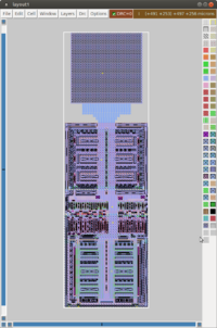
A typical pad cell consists of driver logic, ESD protection and a bonding pad, which essentially just is a "large" metal square, big enough to fit a bonding ball needed to attach the bonding wire or solder it to a PCB (flip chip bonding) or onto another carrier substrate chip (chiplet assembly)
The schematic of the pad cell can generally be broken down into purely combinatory and active analog design components.
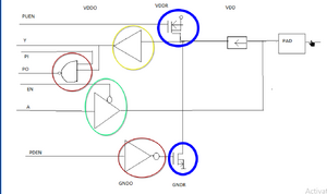
Where we have the two standard logic cells, and inverter and a NAND2 gate (red), transmission gate with level shifting (yellow), a tri-state driver, with 1, 0 and Z (high impedance).(green) and the transistors for pull up and pull down.
Driver Logic
This part of the pad cell is purely combinatorial, and controls based on its pins on the logic side where it's interfacing to the internal logic, what modes should be configured.
For instance, whether the output is enabled, in which case it would either drive current through its driver circuit or pull down to ground in case pull down mode is being set from the internal logic.
It can also be configured for high impedance input, in case OE is disabled.
Various additional functions can be implemented, like for instance impedance and termination resistor calibration in case it's part of a DRAM or PCIe PHY.
In short, the driver logic configures the actual physical properties of the pad depending on what the internal logic tells it to do:
- Set transistors to either drive from the VCC rail to ground or switch towards ground
- Setting whether the driver should be active at all (Output Enable)
- Provide a state engine or other means for configuring the termination resistance to ground.
INV (Inverter)

| Inverter truth table | |
|---|---|
| Input | Output |
| A | NOT A |
| 0 | 1 |
| 1 | 0 |
NAND2 (NAND gate)

| NAND gate truth table | ||
|---|---|---|
| Input | Output | |
| A | B | A NAND B |
| 0 | 0 | 1 |
| 0 | 1 | 1 |
| 1 | 0 | 1 |
| 1 | 1 | 0 |
Input Buffer/Level Shifter
The transmission gate has the purpose of making sure that the input signal is being shifted to the logic levels of the internal logic, for instance 3V3 external logic levels to 1V8 internal logic.
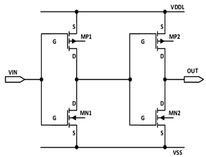
In addition, it contains additional polarity, over voltage and current protection.
Driver circuit
Internally, transistors of a logic circuit only can drive a few micro amperes of current and are unable to survive driving a load like an LED.
In order to make a chip do something useful driver circuits need to be implemented which can provide the power needed for actually driving loads like making an LED blink or driving a small DC motor.
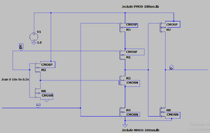
This is being done in the driver circuit through Fingered Transistors which turn the low power logic states at its inputs into a state which is useful to the outside world.
In the schematic above, the output transistors M7 and M8 are responsible for ultimately driving the loads attached to a pad and as such will be much larger than their driving transistors (M1=M6). M7/M8 are Fingered Transistors
ESD protection
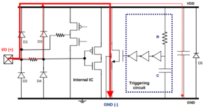
The figure below shows an example of the rail-based protection in which the primary dual diodes (D1 and D2), the secondary dual diodes (D3 and D4), the NMOSFET power supply clamp are employed.
The power clamp provides a current path from the power supply pad to the ground pad during various ESD events.
It's the simplest form of the RC-triggered power supply clamp, where the RC network and the inverter chain are designed such that the NMOSFET (M1) remains off during normal operation and turns on during an ESD event. This NMOSFET should be wide enough to handle the ESD current when it is on during an ESD event.
An example layout found in one of the opened up PDKs available can be seen below
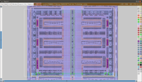
Consult the following literature for more information: http://www-tcad.stanford.edu/tcad/pubs/theses/chun.pdf
Bonding pad
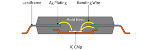
A bonding pad, unlike other components on an ASIC, do not scale down with the feature size, because their area is defined by the physical sizes of the physical solder ball and bonding wire, respectively the solder pads for flip chip bonding required.
Below an example the layout of one of the bonding pads in one of the open PDKs currently available can be seen.
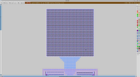
The bonding pad usually is 120x120 and 200x200 microns in size, but there's packaging methods which require even larger pads, like for instance when performing flip chip bonding with a cheap substrate manufacturer.
For flip chip bonding typically an additional layer with isolation oxide and tin pads will be added wiring the output pads to a pad array over the passivization oxide.