Danube River
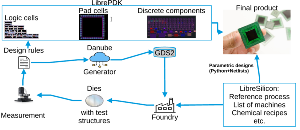
Danube River is a tool, which generates you GDS2 files which you then can manufacture with your prototype process flow in order to validate parameters and adjust your recipes until the values are within a desired range.
Use cases
Setting up a new fab
In case you wanna build a new factory, you basically tape out your Danube River layout over and over again while adjusting the recipes and design rules until the structures aren't broken anymore under the microscope and the values you measure match the predictions you've calculated.
Setting up support for an existing fab
In case you already have a working process and foundry available, but you're not sure that the timing characteristics they've provided are accurate, you can use Danube River for extracting your own timing characteristics.

Successful tapeouts
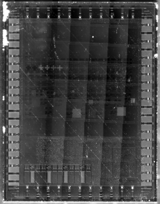
So far, the only opportunity we had to try the new test layout generator, was with Global Foundries on their 180nm node, of which the result can be seen in the picture below:
GDS2 view
The upper left section in the above image corresponds with the layout extracted from KLayout, when opening up the layout used for the tape-out
Structures
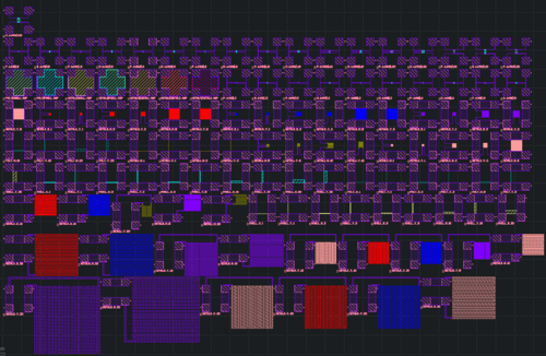
The Danube test wafer has the purpose of allowing to characterize basic analog properties resulting from the manufacturing process flow.
Each of those properties measured can be linked to a specific recipe in the process flow, which allows to fine tune a process and all its process recipes through repeatedly manufacturing and measuring the Danube river layout.
The Danube river contains 3 types of devices, which allows you to determine edge parameters:
- Resistors
- Capacitors
- Transistors
Resistors
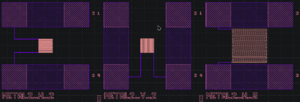
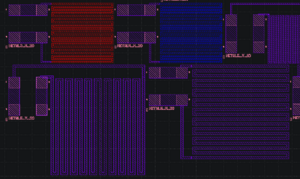
There's three types of resistive test structures on Danube River, due to variations in sheet resistance vs. area and length requirements.
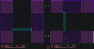
For each sheet resistance characterization there's each a vertical and horizontal configuration in order to catch any potential variance in sheet resistance due to the orientation, which might occur due to the crystal orientation of the substrate being used, like <100>, <110>, and <111>
Strip Resistors
The most simple form of a resistor simply is a straight sheet resistor between pad 1/2 and 3/4 for the vertical sheet resistance characterization and pad 1/4 to 2/3 for horizontal characterization respectively.
Small Meander Resistors
Large Meander Resistors
Capacitors
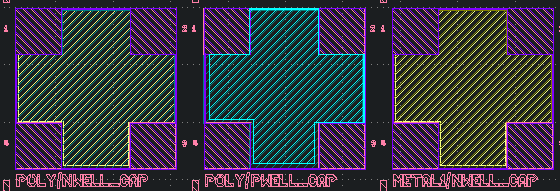
Below some of the capacitors on the test wafer can be seen in more detail.
Transistors
On Danube River there are those very small structures connected the four pads, which for a change aren't connected and configured in a Kelvin configuration, because the pads go to source, drain, gate and bulk each.
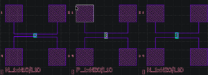
In the closeup below you can see an annotated zoom in onto one of the structures, with each contact being labeled.
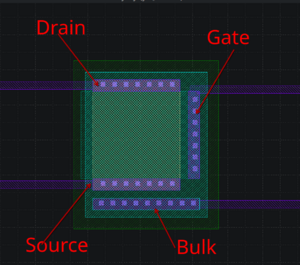
Those structures are probably the most difficult ones to identify.
Measuring method
TODO: Elaborate Kelvin structures